Atmege328 Digital Mppt solar charge controller Project free download

Solar chargers convert solely fifty-five of the solar power, this price loads of star panels. MPPT chargers convert nearly ninety-nine of solar power.
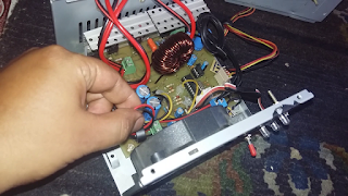
About the Mppt
Well, the foremost advanced star charge controller accessible within the market is most wall socket trailing (MPPT). The MPPT controller is a lot more refined and dearer. It has many benefits over the sooner charge controller. It is thirty to forty yet one more economical at cold. But creating an MPPT charge controller is no bit advanced in comparison to a PWM charge controller. It needs some basic data on power physics. What Is MPPT? Most wall socket huntsman (MPPT) circuit is predicated around a synchronous buck device circuit… It steps the upper electrical device voltage right down to the charging voltage of the battery. The Arduino tries to maximize the watts input from the electrical device by dominating the duty cycle to stay the electrical device operational at its most wall socket. The Maximum wall socket huntsman (MPPT) controller increases charge current by operational the PV module in a very manner that permits the module to supply all the abilities it’s capable of a traditional charge controller merely connects the module to the battery once the battery is discharged. once the 75W module during this example is connected to A battery charging at twelve volts power production is by artificial means restricted to regarding fifty-three watts. This wastes a humongous twenty-two watts or nearly half-hour of accessible power!
The MOSFET Driver: A MOSFET driver permits a coffee current digital signaling from a microcontroller to drive the gate of a MOSFET. A five V digital signal will switch a high voltage MOSFET exploitation of the motive force. A MOSFET incorporates a gate capacitance that you simply ought to charge so the MOSFET will activate and discharge it to modify off, a lot of currents you’ll offer to the gate the quicker you shift on/off the MOSFET, that’s why you utilize a driver.
For this style, I’m employing an IR2104 [*fr1] Bridge driver. The IC takes the incoming PWM signal from the small controller, and so drives 2 outputs for a High and a coffee facet MOSFET. Input: First, we’ve to produce power for the gate driver. It is offered on Vcc (pin-1) and its worth is between 10-20V as per the information sheet. The high-frequency PWM signal from atmega ic goes to IN (pin-2). The finish-off management signal from the atmega ic is connected to SD ( pin 3).
Output: The 2 output PWM signals area unit generated from HI and LO pin. this offers the user the chance to fine-tune the dead-band shift of the MOSFETs. Charge Pump Circuit: The electrical condenser connected between VB and VS together with the diode kind of the charge pump. This circuit doubles the input voltage that the high switch may be driven on. but this bootstrap circuit solely works once the MOSFETs area unit shift
>>>Click here to download the Project for free<<<